We have worked on many projects, and have decided to give you an idea of the process we go through to finalize a project.
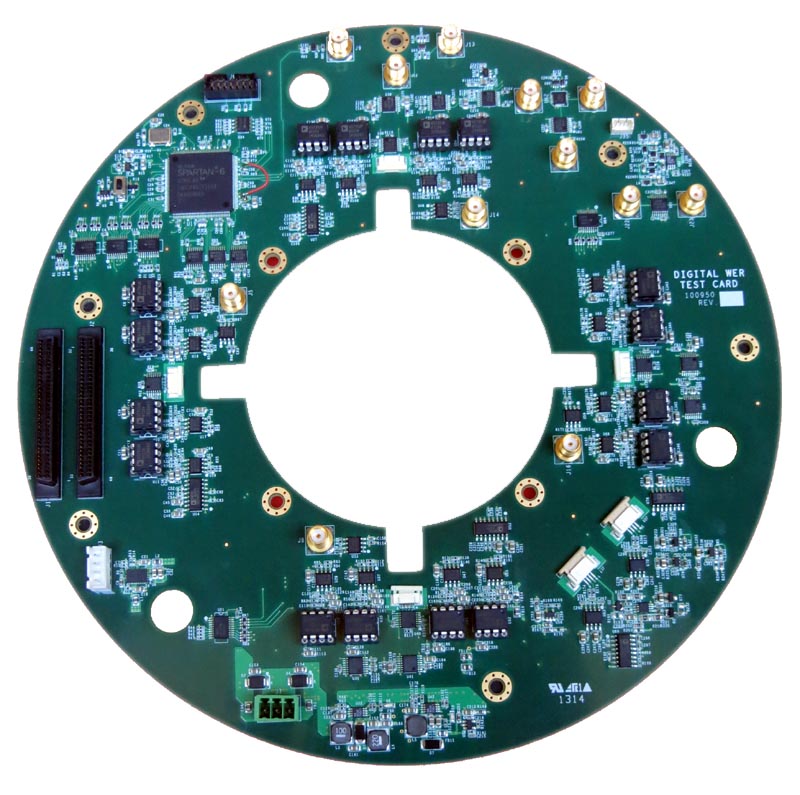
The Digital WER Test card that we have designed is a highly complex, wide function card, which:
- is a test card for an IC maker
- is an 8 layer board, with controlled impedance
- contains almost 1000 components including FPGA
Such a project takes long time to design and finalize. This is how long each step of the project took us:
- Schematic design: 3 weeks (with multiple iterations and reviews)
- PCB layout: 2 weeks
- PCB fabrication: 1 week
- PCB assmelby: 1 week
- First article Bring-up: 1 week
- The Initial FPGA load (verilog) (done during bring-up): 1 week
- After the initial run, there were 3 more production runs.
Our customer received:
- Schematic diagram
- Bill of materials
- Gerber files
- Fabrication drawing
- Assembly files
- Assemlby drawings
- First working board and programming instructions
- Bit file for FPGA and the verilog source code